WAFER Service
6 Inch SiC Wafer Service

Capability
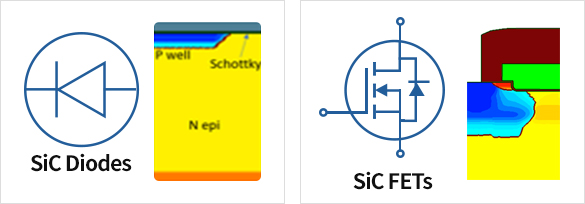
Clean Class : Class 1Custom development and manufacturing for SiC Diode and MOSFET
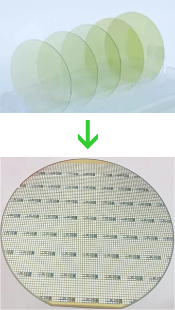
Front-end processing
Photolithography : Resolution 0.4um Trench depth : 3um without micro trench High Temperature Anneal/Oxidation: 2000C/1500C High Temperature implant: 600C
Thinning and back metallization processing
Thinning : 200um Laser anneal : SilicidationSiC Process Capabilities
SiC Process Capabilities
High Temperature Implant ( 600℃ )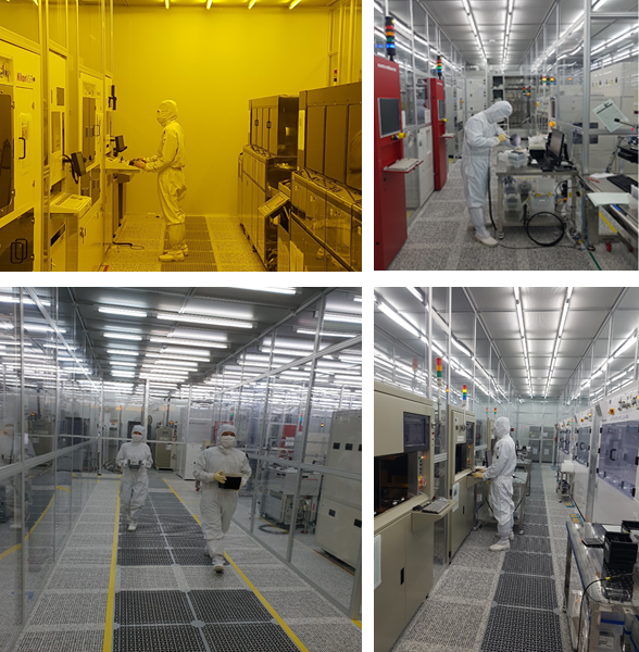
Available Tools for SiC Processing
Photolithography

